Researchers shrink double-slit experiment to atomic scale

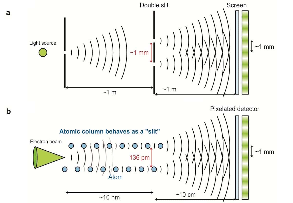
For the first time, physicists in Japan have carried out an atomic-scale version of the double-slit experiment. Using an ultraprecise electron beam channelled along two adjacent columns of atoms in a crystal of silicon, Naoya Shibata and colleagues at the University of Tokyo observed clear interference fringes in electrons scattered by the atoms: fringes that persisted even at high temperature, thanks to correlations in the atoms’ thermal vibrations.
The double-slit experiment is perhaps the most iconic demonstration in quantum mechanics: showing how a single particle’s wavefunction interferes with itself as it passes through two slits at once, with a tangible impact on where the particle is ultimately observed.
In practical research, this effect is now routinely harnessed in electron, neutron and atom interferometers. By observing the interference fringes that it creates, researchers can extract valuable information about both the quantum matter wave and whatever object is doing the diffracting.
Recently, physicists have attempted to push double-slit interferometry all the way down to the atomic scale, replacing conventional slits with crystal lattices. When a moving electron encounters an atom in a crystal, it scatters across a range of angles – producing an outgoing spherical wave that’s mathematically identical to the diffraction pattern from a classical slit.
Since atoms in a crystal sit at such well-defined separations, any neighbouring pair of them could, in principle, act as a double-slit interferometer. In reality, however, the many repeated unit cells in a crystal mean the resulting interference fringes are washed out, making it difficult to isolate the signal from a single atomic pair.
To address this challenge, Shibata’s team used the ultraprecise probe of a 4D scanning transmission electron microscope: an instrument designed to capture electron diffraction patterns with a pixellated detector. Fired into a pure silicon crystal at just the right orientation, the microscope’s precision let the researchers target two adjacent columns of aligned silicon atoms, separated by just 136 pm. As a result, the electron wave overlapped both columns, and no others.
“Our key idea was to use these two atomic columns as the two slits,” describes team member Takehito Seki. “By channelling the probe along both columns at once, we turned them into two coherent scattering sources – effectively making the crystal itself into an atomic-scale double-slit interferometer.”
At this scale, Shibata and Seki’s team created electron interference fringes some seven orders of magnitude smaller than in Thomas Young’s original double-slit experiment with light, first carried out in 1801.
Just as in a larger-scale experiment, these patterns encoded information about the crystal and the electron beam. But at this scale, the researchers could also detect the signature of individual phonon modes in the columns. Rather than destroying coherence as uncorrelated atomic motion would in a classical picture, these correlated vibrations between the two atomic columns kept them moving in sync, preserving the interference.
“In a which-path picture, relative motion of the two atomic columns makes the two electron pathways more distinguishable and reduces the interference, whereas correlated in-phase motion preserves coherence,” Shibata explains. As a result, distinct interference fringes remained visible across temperatures ranging from 300 to 900 K.
The team’s results already point to how an atomic-scale double-slit experiment could offer new ways to measure phonon correlations directly between single pairs of atoms. But as Shibata explains, the possible applications could stretch much further.
“It also opens a route to probing local lattice dynamics at the scale of individual atomic bonds, including at interfaces and defects, where local lattice dynamics can strongly influence thermal transport,” he says. “In the long run, such atomic-scale insight could help inform better thermal management strategies for future chip technologies.”
The study is published in Nature.
The post appeared first on Physics World.

 点赞
点赞 收藏
收藏 点踩
点踩 分享
分享