Hot Chips 2026: Intel's Wildcat Lake – By Chester Lam

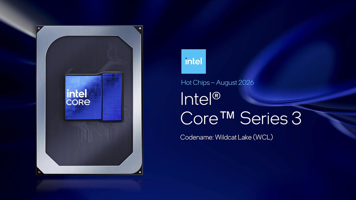
Intel’s Core Ultra series has done well with improving battery life and performance in mobile products. Wildcat Lake, or Core Series 3, aims to take those qualities and bring them into a lower cost product. Wildcat Lake brings in all the new technologies present in the Core Ultra series, rather than making an incremental change off the N and U series that had filled out Intel’s past low cost offerings. That includes new IO, new CPU cores, and the Xe3 graphics architecture for the GPU. But optimizing for low cost goes beyond taking those major IP blocks and picking the right core counts. That’s what Intel’s presentation is about.
Intel’s Ultra-series processors use advanced packaging technology to avoid creating a large, difficult-to-yield monolithic die. As far back as Meteor Lake, Intel has been using small dielets that yield better. Core Ultra 3 in the more recent generation features two different compute dies and two graphics dies that can be mixed and matched as needed. That scheme was great for flexibility and validation, but the low cost segment doesn’t need that kind of flexibility. Intel found that as they right-sized their IPs, they wound up with smaller dies that didn’t need so much breaking up. Multiple compute die or graphics die variants didn’t make sense either, because the low end doesn’t need configuration flexibility beyond what binning a single compute die can do. Advanced packaging also incurs cost. Intel saw that for their target price points, they either needed to use a monolithic die, or go MCP. They chose the latter (MCP).
Then, Intel decided to use a unique platform rather than reuse the Core Ultra platform. Final product cost includes partner BOM costs on top of the SoC cost, and using a different platform opens up more cost reduction opportunities. One example is using a narrower memory bus running at a higher data rate, which turned out to enable large BOM savings.
In some areas, Intel kept features in even though they increased cost because of how important they were to battery life. Wildcat Lake continues to use separate power rails for the LPE cores and iGPU. Intel also continues to integrate support for the latest WiFi and Bluetooth standards, which means OEMs don’t have to spend on separate controllers.
Intel curiously went in the opposite direction for the camera by removing built-in camera support. Intel mobile CPU SKUs going back to Skylake integrated an Image Signal Processor, or ISP. ISPs take raw input from a camera, and turn that data into a usable image by accounting for the color filter array pattern (de-bayering), applying exposure and contrast adjustments, and so on. Wildcat Lake doesn’t feature an ISP. Intel found that a lot of OEMs implemented USB ISPs, so taking the dedicated camera interface out made sense.
Wildcat Lake’s display engine has three pipes, compared to the four typically found on higher end Intel parts. Display pipes in Intel’s display engine generally each drive a display, with small exceptions like joining pipes to drive 8K panels. The cutback means Wildcat Lake can only drive three displays. Intel also limited resolution support to 4K 60 Hz. Consumers are unlikely to get a budget SoC to drive 8K panels or quad-display setups, so Intel’s display engine downsize makes sense. Supporting the display bandwidth required for 8K would also have created challenges at the UCIe link.
Battery life is of paramount importance to a display engine, because displays have to work even when the CPU and GPU are idling. A lot of display power optimization comes down to letting various buses and interfaces sleep for as long as possible, instead of constantly trickling data through. At the display engine’s “frontend” (my term for simplicity), Intel has long used a display buffer to enable bursty reads from DRAM. Doing so lets the memory controller sleep between bursts. That remains important in Wildcat Lake, because a lot of budget devices don’t have displays with panel self-refresh capabilities. Without panel self refresh, the display engine has to constantly send new frames out even when nothing has changed.
Optimizing for constantly refreshing the display extends to the display engine “backend”. There, Intel added a new buffer after the display pipes generate the composited output. This buffer carries out a similar optimization to the frontend display buffer, but targets the UCIe interface rather than the memory controller. Scheduling traffic in bursts lets the UCIe interface transition to lower power states.
UCIe Considerations
Display engine optimizations for UCIe are important because UCIe is more costly in area and power terms than the Foveros interface used in Intel’s higher end Ultra parts. Foveros uses a very fine bump pitch, which allows for wide, low-clocked interfaces run directly between dies. UCIe is a packet-based protocol with a larger bump pitch, and doesn’t run through a base die. The interface by itself therefore consumes more power and area. On top of that, the packet-based nature of UCIe means it needs controller logic to convert interface signals into that packet format. The UCIe controller comes with an additional power and area cost, which also requires attention to control cost and power draw.
Beyond the display engine, Intel right-sized IO for mainstream consumers. They provisioned 12 GB/s of UCIe bandwidth to support a typical configuration with a PCIe 4.0 SSD with some headroom to spare. A user can theoretically hit limits if they max out SSD bandwidth while also creating heavy IO load elsewhere, for example by hitting the USB subsystem hard. However, such concurrent high IO load is extremely rare for consumer use cases.
All of this IO right-sizing lets Intel run the UCIe interface at 8 GT/s. 8 GT/s is modest compared to UCIe 2.0’s maximum 32 GT/s, or UCIe 3.0’s 64 GT/s. However, running at that lower data rate keeps the raw bit error rate low. Intel took advantage of that low error rate to dispense with retry and forward error correction mechanisms. Intel noted that for the display, there’s really no backing out of a flow anyway.
Cross-die protocols are difficult to validate, and validation is part of the engineering cost that factors into final product cost. Intel therefore sought to ensure “survivability”. Anything that could be a fuse was made a fuse, or at least a configuration register that could be written very early. Presumably, that lets Intel chicken-switch their way out of paths that turn out to have late-stage bugs. Packetized sideband signals also get a get-out-of-jail free card with an alternate mechanism that can mux them down to a single spare pin (and get demuxed after). Intel can take up to four packetized signals and change them back to single ended.
Down-sizing Xe3
Budget conscious consumers buying Wildcat Lake products aren’t looking for high GPU performance, so Intel chose a conservative iGPU configuration with two Xe cores. To further save area, Intel removed hardware raytracing acceleration. This move is sensible considering that mobile GPUs don’t have enough processing power to run games at high resolutions and settings. Raytracing is basically an extra-ultra setting, and would be difficult to take advantage of in a low cost, low power platform.
Intel also thought about removing systolic arrays for matrix multiplication in the Xe Cores, but decided to keep them in. That turned out to be a good decision, because the combination of matrix multiplication units in the GPU, ones in the NPU, and CPU compute throughput lets them reach roughly 40 TOPS.
Die Recovery
As with all Intel products, Wildcat Lake tries to maximize yields by creating several SKUs. Fabricated IP ends up on a frequency distribution where not all parts can meet required specifications for a given SKU. Intel therefore bins for different clock speeds, and can disable blocks with defetcs. That’s typical practice for consumer products.
Intel however took care to avoid binning that would create SKUs no one wants, or would create too much complexity. For instance, they looked at harvesting LPE cores, but decided not to because a product without LPE cores might compromise battery life. Harvesting display pipes or IO falls into a similar bucket, because having products that can’t drive three displays or have USB capabilities that OEMs planned for but can’t use isn’t great. Remember that Wildcat Lake doesn’t have a built in ISP, so some USB has to be allocated for the webcam typically found in mobile devices.
Final Words
The current economic trend is for income to stagnate while product costs tend to outpace inflation and AI advances drive strong growth in utility bills. That trend makes low cost products especially exciting, and Wildcat Lake has been a fascinating look at how Intel is trying to make a sensible low cost SoC. Typical consumer chips have a lot of processing power and IO capabilities that are rarely used. Trimming the fat creates a sensible product that’ll likely deliver adequate performance for a very wide audience. Right-sizing each component can uncover more costs savings while keeping the product balanced. While not mentioned, I imagine moving to a 64-bit memory interface makes sense with a smaller iGPU and lower core count. High DRAM bandwidth demands tend to come either from high performance GPUs, or from highly parallel CPU loads that scale across cores. Wildcat Lake isn’t optimized for either case, so using a wider DRAM interface would just mean a very under-utilized memory bus.
Wildcat Lake instead focuses on the most important areas that everyday applications will feel. Compared to Intel’s N350 for example, Wildcat Lake Core Series 3 moves away from the dated Gracemont architecture on Intel 7 and goes straight to Intel 18A with Lion Cove and Skymont. It’s not a halo product meant to compete in the most expensive devices around, but it brings in the most essential goodies from Intel’s higher end line while keeping battery life in focus. It’ll be nice to see low end devices that feel good to use without breaking the bank, and Wildcat Lake is an exciting development on that front. Hopefully, Intel’s experience gained with developing this product feeds into strong follow-up chips in the same segment.

 点赞
点赞 收藏
收藏 点踩
点踩 分享
分享