Hot Chips 2026: Samsung and HBM Base Die Opportunities

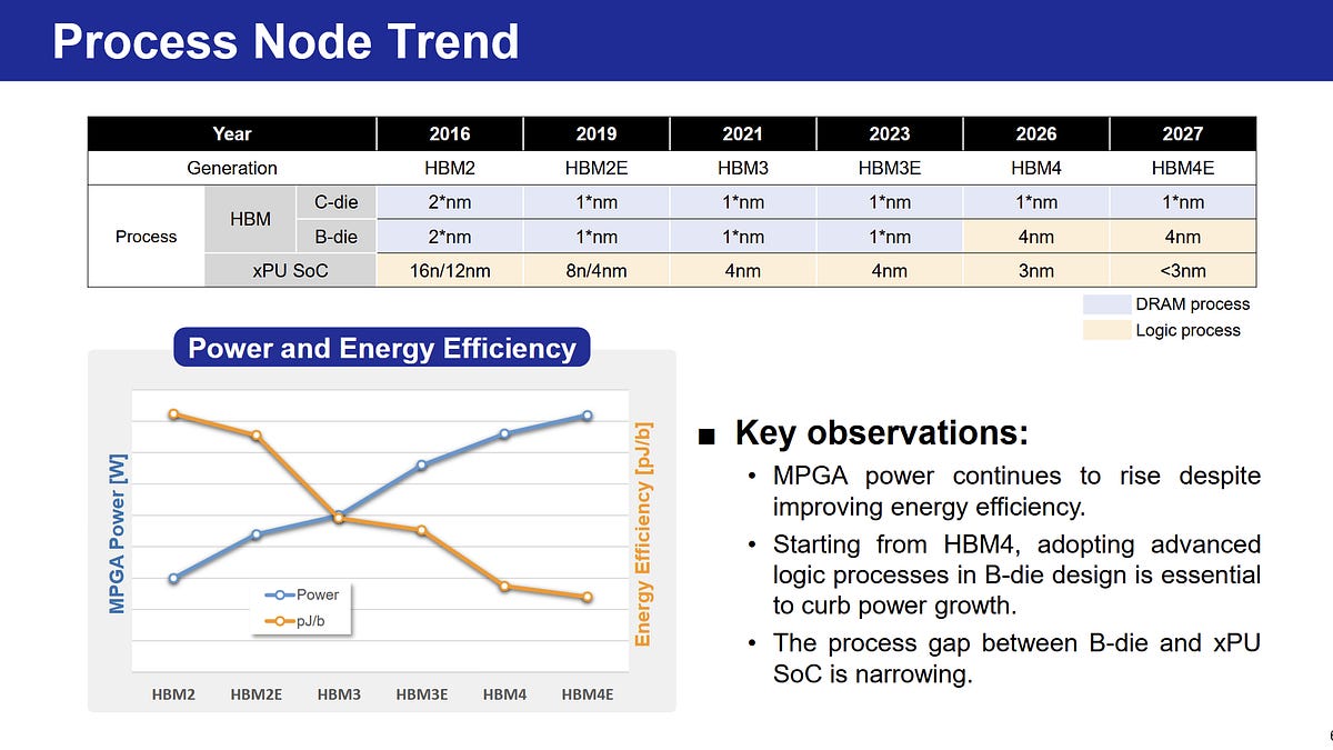
HBM, or High Bandwidth Memory, stacks multiple DRAM dies on top of a base die. The dies interface with each other via TSVs, while the base die talks with whatever compute die is using the memory via an interposer. Increasing bandwidth for a new HBM generation involves scaling up bandwidth between the DRAM dies and the base die, as well as scaling bandwidth from the base die to the host. Denser TSVs and more TSVs can easily achieve the former. The latter is more challenging, because the physical interface between the base die and host is already the biggest consumer of base die area. Increasing data pin count makes the area problem worse, and is bad for power consumption. Samsung notes that even though each HBM generation improves power efficiency, memory power keeps going up.
Samsung answered this challenge by switching to a logic node, moving away from fabricating the base die on a DRAM node. HBM4 and HBM4E now use their 4nm logic process. A logic node helps mitigate power draw increases, and offers improved density that opens up other optimization opportunities. After moving to a logic node, Samsung found they had a lot of unused base die area. They can’t make the base die smaller because its area is dictated by the DRAM die stacked on top, so they’re looking at opportunities to use that area to do fun things. Samsung’s presentation goes over those opportunities, split into three phases.
Phase 1 investigates moving the memory controller onto the HBM base die. DRAM conventionally is rather “dumb”, requiring a host memory controller to manage low level details like precharging rows, switching the bus between read and write mode, and refreshing DRAM cells. The memory controller receives basic requests for data (give me data from this address), queues up those requests, and tries to schedule them to maximize performance while preserving correctness around memory ordering. Samsung wants to bring those functions onto the base die, and use a custom die-to-die interface to the compute die instead of the standard HBM interface. By doing so, Samsung hopes to reduce PHY area on both the compute and HBM base die. Saved PHY area could be used to hold the memory controller, making the move essentially free from the HBM base die’s perspective.
If Samsung pulls this off, you could imagine a hypothetical product working like Intel’s Sapphire Rapids, but with HBM dies that directly understand the mesh protocol internal to the CPU. A tradeoff might be that custom HBM requires more integration effort, because it no longer talks to a standard memory controller. Samsung could try to standardize a custom protocol to get around this, though their exact plans remain to be seen.
Samsung is also looking at integrating a block of SRAM into the base die that stores remapping information to get around failed DRAM cells. Previously this was done at the DRAM dies, but that has limited flexibility. Presumably, row spares can only be used to replace defective rows on the same die, and ditto with column spares. A SRAM-based remapping table could use individual cells in row/column spares to replace any defective cell. It’s also easy to imagine spares on one die being used to replace defective cells on another.
Phase 2 looks at reclaiming even more unused base die area, because apparently there’s room left even after integrating the memory controller. Samsung wants to integrate more sensors, letting HBM provide better telemetry around temperature and voltage. To improve yields and test coverage, die area can be used for a test block. This test block generates test patterns, working a bit like memtest but without needing a host.
Memory expansion was also discussed as part of phase 2. The base die can interface with external memory, acting as an IO die of sorts. No one can seem to get enough memory capacity, and HBM capacity can be limited by interposer/chip size. Putting external memory PHYs on spare HBM base die area could be an attractive way to connect a compute die to even more memory.
In-memory compute makes an appearance as part of phase 2 as well. Spare area can host compute. I’m skeptical of near-memory compute because that compute is tied to a region of memory. It would suffer from all the challenges of NUMA setups, but in a more severe way because each PE integrated onto the HBM base die is unlikely to have large caches capable of holding data homed to other memory dies. Perhaps it can be useful for pre-processing data, like performing format conversions as data gets loaded into the compute die’s internal storage.
Phase 3 goes after more aggressive solutions. Samsung is looking stacking HBM dies on top of a compute chip, a bit like how mobile SoCs stack memory using package-on-package form factors. I suspect thermals will be a huge challenge. AMD spent several generations improving thermals with their 3D cache stacking. Zen 3, Zen 4, and Zen 5 all saw their stacked cache variants clock significantly lower than their vanilla counterparts, and that’s with a single die on top. HBM will stack many more dies, further complicating the cooling
If thermals do work out, this zHBM solution could offer all the potential benefits of 3D stacking. TSVs don’t take as much power or area as 2D PHYs. Any power or area saved can be given back to more compute, assuming that compute doesn’t create hotspots that are difficult to cool through a pile of HBM die layers.
Final Words
Samsung and other memory manufacturers are investigating a lot of exciting possibilities with HBM, undoubtedly driven by the explosion in DRAM demand. Many of Samsung’s proposals revolve around more tightly coupling DRAM with the compute using it. They may be difficult to achieve if compute chip makers want to multi-source HBM, because then Samsung will have to get other DRAM vendors on-board with its custom solutions. Some of Samsung’s phase 1 goals look very achievable. Better on-die test and RAS facilities, for example, wouldn’t need special attention from an attached compute die. Phase 2 and phase 3 stuff looks like a stretch. Whatever happens, it’ll be exciting to see.

 点赞
点赞 收藏
收藏 点踩
点踩 分享
分享